Field -effect transistor (FET) it’s a unipolar, semiconductor device like BJT. FET stands for Field Effect Transistor. FET is the voltage controlled device as we know BJT is current control device. Its unipolar device have high switching speed & high cut off frequency as BJT is bipolar device low switching speed & low cut off frequency. The field effect transistor offer many feature and application in analog switching, amplification, microwave amplifier etc. The Field effect transistor (FET) is a three terminal device those are
A. Drain (D): Accept coming voltage & current from source.
B. Source (S): Source of voltage & current towards Drain
C. Gate (G): Gate terminal acts as a controlling terminal of source and drain control flow of Voltage & Current.
It’s very important to know what difference between FET and BJT as well as some similarity that will be consider as follow :
Sr.No Parameter BJT JFET
1. Voltage Gain (Vg) High Voltage Gain Low Voltage Gain
2. Current Gain (Ai) Low Current gain High current gain
3. Input Impedance (Zi) Low input impedance Very high input impedance
4. Output impedance(Zo) Low output impedance High output impedance
5. Noise Medium Noise Generation Low Noise Generation
6. Switching Time (Ts) Medium switching time Fast switching time
7. Turn off Requires zero input Some need an input to turn it "OFF"
8. Control Parameter Current controlled It is a Voltage controlled device.
9. Cost Cheap More expensive than BJT.

Construction and symbol of N-channel JFET

Working Principle of N-channel JFET
First Phase:
(No Vs with terminal): When neither any bias is applied to the gate i.e. when VGS = 0V and no any voltage is applied to the drain to source i.e. VDS = 0, the depletion region are of equal thickness and symmetrical.
Second Phase:
(Vs = Vgs=0&Vds≠0): When positive voltage is applied to the drain to source terminal without connecting gate terminal G to supply, the electrons starts to flow from Source to Drain and drain current ID flows through the channel N from Drain to Source. Due to flow of this current, there is uniform voltage drop across the channel resistance as we move from terminal D to terminal S. This causes the reverse biases of diode. The gate is more “negative” with respect to those points in the channel which are nearer to D than to S. Hence, depletion layers penetrate more deeply into the channel at points lying closer to D than to S. The size of the depletion layer formed decides width of the channel and hence the magnitude of current ID flowing through the channel.
Third Phase:
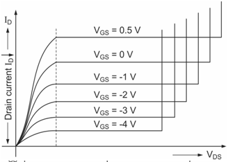
consider the gate G is negative biased with respect to the source S while the drain is applied with positive bias with respect to the source. This is shown in the figure. The P-N junctions are then reverse biased and depletion regions are formed. P regions are heavily doped compared to the N-channel, so the depletion regions penetrate deeply into the channel. Since a depletion region is a region depleted of the charge carriers, it behaves as an insulator. The result is that the channel is narrowed, the resistance is increased and drain current ID is reduced. If the negative voltage at the gate is again increased, depletion layers meet at the center and the drain currents cut-off completely.
Fourth Phase:
If the negative bias to the gate is reduced, the width of the depletion layers gets reduced causing decrease in resistance and , therefore, increase in drain current ID.(The gate-source voltage VGS at which drain current ID is cut-off completely (pinched off) is called the pinch-off voltage Vp. It is also to be noted that the amount of reverse bias is not the same throughout the length of the P-N junction. When the drain current flows through the channel, there is a voltage drop along its length. The result is that the reverse bias at the drain end is more than that at the source end making the width of depletion layer more at the drain. To see how the width of the channel varies with the variation in gate. Consider the figure above understand concept.


No comments:
Post a Comment